

Take a look at our newest merchandise


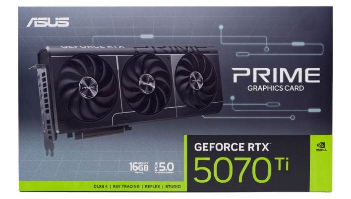
| ASUS PRIME GeForce RTX 5070 Ti: MSRP $749 The GeForce RTX 5070 Ti brings NVIDIA’s newest Blackwell GPU structure all the way down to a $749 beginning worth level, with out sacrificing any options, but it surely’s not an enormous improve over the earlier gen.
|
|||

|


|
||
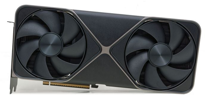
NVIDIA continues its onslaught of Blackwell-based GeForce RTX 50 sequence playing cards right this moment, with the discharge of the GeForce RTX 5070 Ti. Technically, playing cards go on sale tomorrow from NVIDIA’s board companions, however over the subsequent couple of days we are able to present you what a few the playing cards can do by way of efficiency, beginning with the ASUS PRIME GeForce RTX 5070 Ti we’ll be that includes right here.
Like the entire different GeForce RTX 5070 Ti playing cards coming down the pipeline, the ASUS PRIME contains a proprietary design with ASUS’ personal tackle NVIDIA’s upper-midrange GPU, however this specific mannequin must be arriving at NVIDIA’s specified $749 MSRP – an ASUS PRIME GeForce RTX 5070 Ti OC Version, with considerably increased enhance clocks can be coming, and might be considerably costlier. The identical is true for numerous different producers that might be providing a number of fashions at or above MSRP.
Earlier than we dive in and get up-clos-and-personal with the ASUS PRIME GeForce RTX 5070 Ti although, let’s lay among the groundworks and clarify the place the RTX 5070 Ti lives in NVIDA’s line-up. Specs and a fast comparability up first…
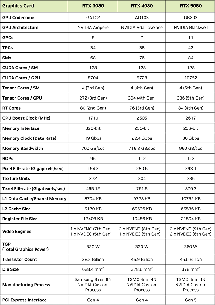
NVIDIA GeForce RTX 5070 Ti Specs
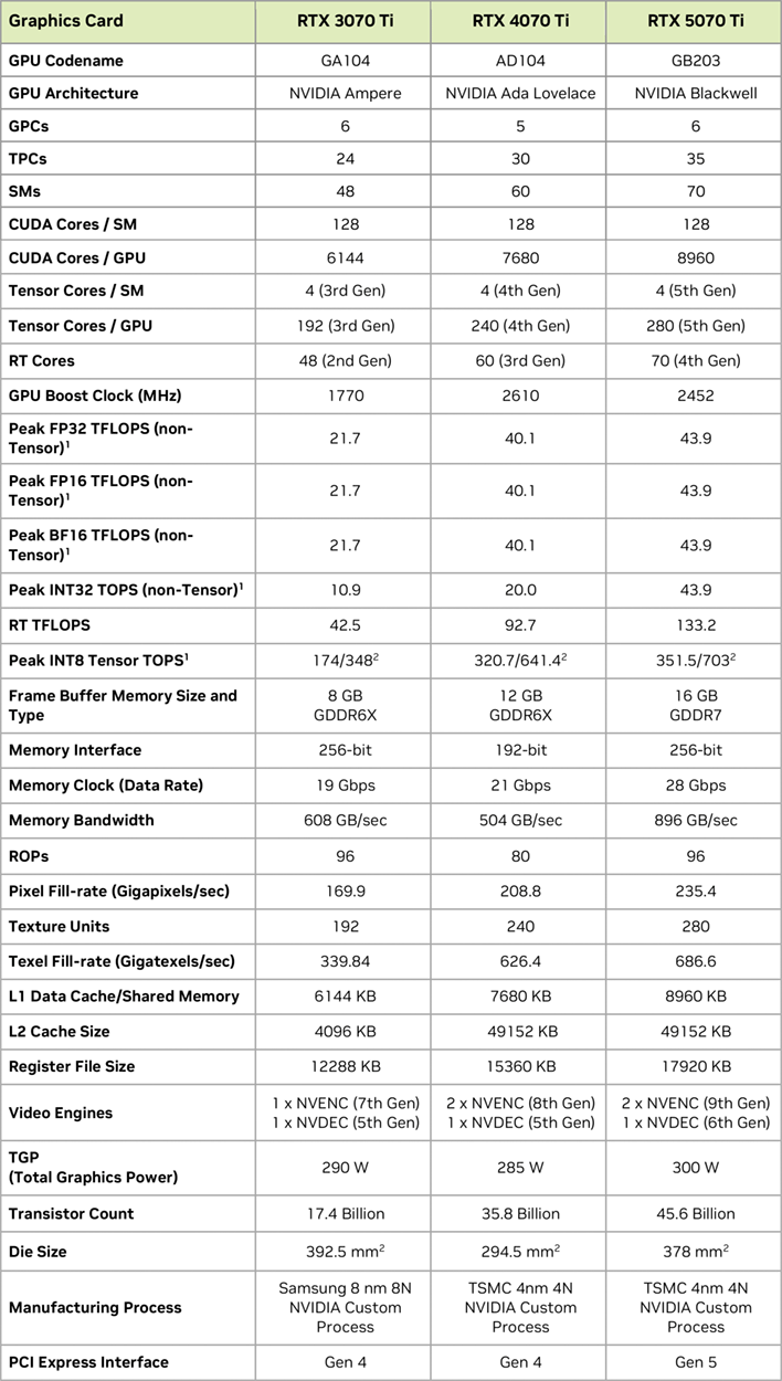
The above desk compares the principle options and specification of the final three “70” class GPUs from NVIDIA. As you may see, by way of its specs, the GeForce RTX 5070 Ti is an improve over the previous-gen GeForce RTX 4070 Ti in most methods. The GeForce RTX 5070 Ti has extra cores, that are additionally primarily based on a more moderen structure, extra reminiscence with a lot increased bandwidth, extra L1 cache, a bigger register file, an upgraded media engine, a local PCIe Gen 5 interface, and better pixel and texture fill charges, regardless of a considerably decrease enhance clock. Just like the RTX 3070 Ti, a 256-bit reminiscence interface returns, which leads to almost 900GB/s of peak bandwidth when paired to its speedy 16GB of 28Gbps GDDR7 reminiscence.
Just like the GeForce RTX 5080, the brand new RTX 5070 Ti is constructed across the 45.6 billion transistor GB203 GPU. However not like the GeForce RTX 5080, which contains a full-fat chip, the RTX 5070 Ti is scaled again considerably. The complete GB203 as it’s configured on the RTX 5080 options 11 GPCs, 42 TPCs, 84 SMs, and eight 32-bit reminiscence controllers, for an combination 256-bit bus width. Every SM accommodates 128 FP32 CUDA Cores, for a grand whole of 10,752, with 84 4th Gen RT Cores, 336 fifth Gen Tensor Cores, 336 Texture Items, and 112 ROPS. The GB203 additionally features a whole of 10,752 KB L1 cache, a 21,504 KB Register File, and 65,536 KB L2 cache. On the GeForce RTX 5070 Ti, nonetheless, solely 6 GPCs, 35 TPCs, and 70 SMs are enabled, which leads to 8,960 whole CUDA cores, 280 Tensor cores, and 70 RT cores. The L1 cache commensurately drops down to eight,960KB, with 49,152KB of L2 as nicely.
Whereas the GB203 powering the GeForce RTX 5070 Ti is scaled again versus the extra highly effective GeForce RTX 5080, or GeForce RTX 5090 for that matter, its options and capabilities stay the identical. RTX Neural Rendering, RTX Mega Geometry, DLSS 4 with Multi-Body Gen, the brand new AI Administration Processor, and up to date media engine with {hardware} acceleration for 4:2:2 video, are all a part of the GeForce RTX 5070 Ti’s characteristic set. You possibly can find out about all of these options in our earlier NVIDIA Blackwell GPU structure protection, if you have not already learn it.
Examine Out The ASUS PRIME GeForce RTX 5070 Ti
|
|
NVIDIA GeForce RTX 5080 Founders Version: MSRP $999
The NVIDIA GeForce RTX 5080 Founders Version appears to be like similar to the flagship RTX 5090, and presents the identical options, however packs a smaller GPU at solely half the worth.
|
|
|
|
|
|
|
|
Though the RTX 5080 Founders Version card we’ll be displaying you right here appears to be like primarily an identical to the RTX 5090, there are many variations underneath the hood. Actually, the playing cards aren’t even constructed utilizing the identical GPU. Extra on that in a bit.
The NVIDIA GeForce RTX 5080 Founders Version’s packaging and bundle is strictly the identical because the RTX 5090’s. In stead of writing about the entire environmentally pleasant and sustainable goodness in NVIDIA’s newest packaging once more, we’ll let Davo inform you instantly. Take a look at the video above to see for yourselves – simply think about that 9 is an 8…
NVIDIA GeForce RTX 5080 Specs
The GeForce RTX 5080 is constructed across the 45.6 billion transistor GB203 GPU, however not like the RTX 5090, which has a scaled again GB202 at its coronary heart, the GeForce RTX 5080 contains a full-fat chip. The GB203 is supplied with 11 GPCs, 42 TPCs, 84 SMs, and eight 32-bit reminiscence controllers, for an combination 256-bit bus width. Every SM accommodates 128 FP32 CUDA Cores, for a grand whole of 10,752 CUDA Cores, with 84 4th Gen RT Cores, 336 fifth Gen Tensor Cores, 336 Texture Items, and 112 ROPS. NVIDIA’s GB203 additionally contains 10,752 KB L1 cache, a 21,504 KB Register File, and 65,536 KB L2 cache. The GPU is linked to 16GB of GDDR7 reminiscence working at an efficient 30Gbps, for as much as 960GB/s of bandwidth.
Examine Out The NVIDIA GeForce RTX 5080 Founders Version
By way of its industrial design and general aesthetics, the GeForce RTX 5080 Founders Version LOOKS similar to the RTX 5090 FE. There are some key variations we must always be aware, nonetheless.
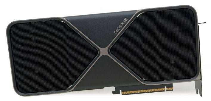
Just like the GeForce RTX 5090, the GeForce RTX 5080 is way thinner than its direct predecessor. The cardboard measures 304mm in size, 137mm in top, and it’s really two-slots (40mm) huge – it’s not only a 2-slot case bracket, with a protruding cooler meeting. It is a dense package deal that makes use of premium supplies through-and-through. You possibly can really feel the construct high quality as quickly as you decide up the GeForce RTX 5080.
NVIDIA was in a position to shrink its top-end GeForce RTX 50 sequence playing cards this technology by growing what it calls a “Double Move Via” cooler design, which permits each cooling followers to blow air straight by way of the heatsink, for optimum efficiency with decreased noise.
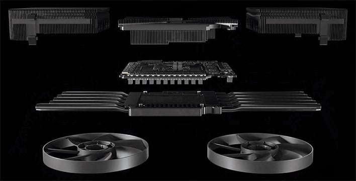
To attain this, the GeForce RTX 5080 has a multi-part PCB setup, just like the 5090’s. The central PCB is dwelling to the GPU, reminiscence, and energy circuitry. It’s located within the heart of the cardboard, with solely small parts protruding beneath every fan. A separate daughterboard attaches to the central PCB to the PCIe x16 connector, and a 3rd, versatile board runs perpendicular alongside the underside edge with high-speed signaling connections from the central PCB to the show outputs.
The GeForce RTX 5090 has a newly-designed 3D Vapor Chamber affixed to its GPU, reminiscence and energy circuitry for cooling functions, with a liquid steel TIM to assist in warmth switch. The GeForce RTX 5080, nonetheless, has a extra conventional chilly plate, with a dense array of heatsink thin-fins, linked by way of 5 warmth pipes — it’s not outfitted with the identical vapor chamber because the 5090. NVIDIA additionally makes use of a extra conventional phase-change TIM on the RTX 5080, so not one of the complexities related to liquid steel are at play right here. Externally although, you may’t actually inform. The identical twin axial followers are current, together with the identical directional shops on the heatsink and prime and backside vents on the shroud.
Outputs within the GeForce RTX 5080 (and different RTX 50 sequence playing cards) mirror the RTX 5090 as nicely, and embody a trio of DisplayPorts (2.1b) and a single HDMI port (2.1b). Their orientations have been reversed versus previous-gen playing cards although, and the case bracket contains a strong entrance bezel and an anti-fingerprint coating.
Now that you just’re intimately conversant in the GeForce RTX 5080’s design, let’s get to the benchmarks…
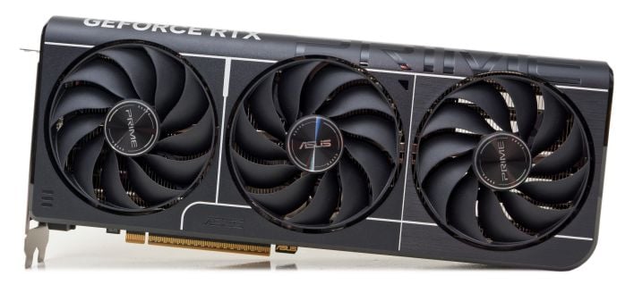
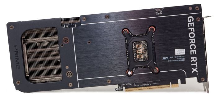
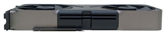
Dominating the entrance of the ASUS PRIME GeForce RTX 5070 Ti is triple-fan cooling resolution, with curved edges and a partial pass-through design. The cardboard options twin ball fan bearings for added sturdiness, with what ASUS calls “Axial-tech” followers. That principally means the fan hub is a bit smaller and the fan blades are a bit longer than typical axial followers, which reduces noise, will increase downward stress, and in the end improves cooling efficiency.
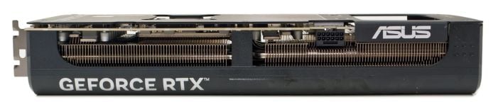
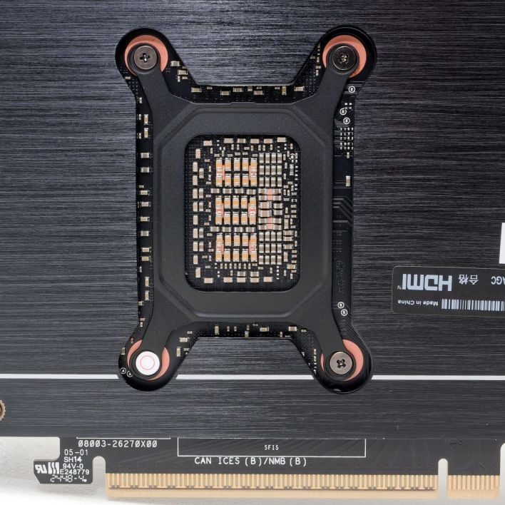
The heatsink underneath these followers covers the whole PCB and extends off the again a couple of inches to allow the aforementioned partial pass-through design. The heatsink makes direct contact with the GPU, reminiscence, and voltage regulation circuitry on the ASUS PRIME GeForce RTX 5070 Ti, and the corporate claims the bottom of the heatsink is machined with increased precision than competing playing cards, to enhance contact space and warmth switch. ASUS additionally makes use of a phase-change GPU thermal pad, which the corporate claims improves thermal conductivity underneath heavy load. At any fee, the cooler is greater than succesful and retains the GB203 on this card operating cool, even whereas overclocking. The ASUS PRIME GeForce RTX 5070 Ti can be good and quiet, however we’ll talk about thermals and acoustics in additional element a bit later.
The ASUS PRIME GeForce RTX 5070 Ti additionally contains a vented steel backplate, and a dual-BIOS swap labeled with a “P” and “Q”, we supposed for efficiency and quiet modes, however ASUS’ website lists “default” and “OC” modes. Regardless of the modes are literally referred to as, the cardboard’s default GPU enhance clock is 2,452MHz (when the swap is ready to Q). That clock will increase barely to 2,482MHz when in P-mode, nonetheless.
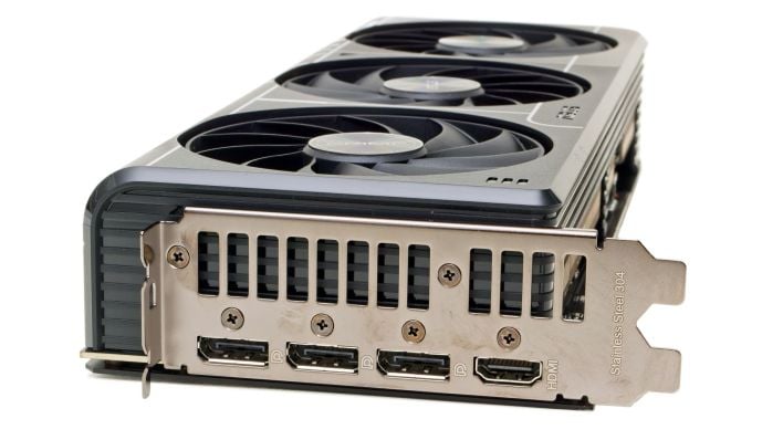
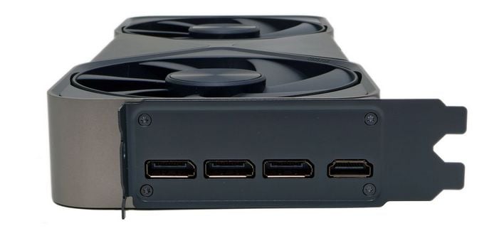
Outputs within the ASUS PRIME GeForce RTX 5070 Ti mirror different GeForce RTX 50 sequence playing cards and embody a trio of DisplayPorts (2.1b) and a single HDMI port (2.1b). These ports are nestled into a stainless-steel backplate, that options venting for some odd motive, as a result of the plastic fan shroud behind these vents is strong.
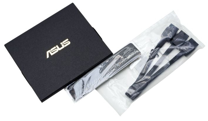
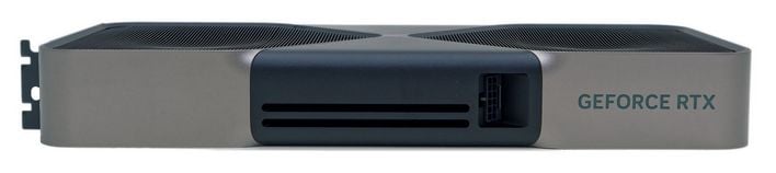
Included with the ASUS PRIME GeForce RTX 5070 Ti is a primary lit pack, a thanks card, a single strip of hook & loop fastener, and an influence adapter that takes three 8-pin PCIe Specific energy feeds and converts them to a single 12VHPWR connector.
And with all of that coated, let’s get to some benchmarks…
![[2024] MSI Aegis R2 C14NUF9-829US (Intel Core i9-14900F, 128GB DDR5 RAM, 2X 2TB NVMe SSD, NVIDIA GeForce RTX 4070 Ti Super, Windows 11) Gaming Desktop PC](https://m.media-amazon.com/images/I/81i1KVslX4L._AC_SL1500_.jpg)